Analysis of Filter Deposits, Chip Detector Deposits, Corrosion Deposits, Separated Solids in Lubricants,
Conductive or non-conductive materials,
Magnification up to 10,000 times,
Detection of more than 90 elements,
Color images show the distribution of elements,
EDS for analysis of composition,
Photographic display,
Composition display,
Dimensions in μm or mm,
Quick Turnaround.

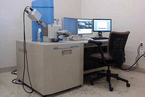
Metro Tech Systems now offers surface imaging and chemical analysis on a variety of materials including filter or aircraft chip detector debris, corrosion deposits, and separated solids in lubricants using our JEOL Scanning Electron Microscope (SEM). Our Scanning Electron Microscope is equipped with an Energy Dispersive Spectrometer (EDS), allowing us to provide a chemical analysis of the field of view, or spot analysis of minute particles. Using the SEM/EDS method with our low-atomic number detectors, we can determine the composition and quantification of more than 90 elements with a presence of more than 0.1% in a homogeneous sample.
The SEM has a greater depth of field than traditional light operated microscopes which allows more of the object to be in focus at one time. Images are generated using backscattered and secondary imaging. The SEM also has much higher resolution allowing closely spaced particles to be magnified at much higher levels. Images up to 10,000 times the size of the particle can be produced with extraordinary clarity. The SEM is capable of viewing both conductive and non-conductive samples. The images provided show the patterns, groves and cracks within the material that can then be used for further analysis. The high-resolution, three-dimensional images produced by the SEM provide topographical, morphological and compositional information of the object. Particle sizes can be measured in terms of μm or mm.
For further information, click on the link below
SEM-EDS Information Request
